On 2026-06-30, c186282 <c186282@nnada.net> wrote:
On 6/30/26 09:51, Mr. Man-wai Chang wrote:
On 6/30/2026 5:14 PM, c186282 wrote:
Can you fabricate 0.000000...0000000001 nm chips?
Is zero the seal or wall? :)
ÿÿÿ Um, pretty quick you get to ATOMS ... and, for any
ÿÿÿ normal electronics, that's IT.
You cannot have 0.000000....00 nm chip.
That's a void, empty, nothing. :)
I tried to think through the implications of this
but I got a divide error.
"Electronics" are now about literal atom-thick structures.
Can't go any smaller.
Any better future stuff will have to exploit quantum
effects - get more bang for yer nanometer. Alas quantum
stuff isn't as deterministic as bulk matter devices
and suffer from the uncertainty principle.
Omigod, we might have to revive the KISS principle
in order to get anything more done. The proponents
of complexity as a weapon will be so disappointed...
On 6/30/26 09:51, Mr. Man-wai Chang wrote:
On 6/30/2026 5:14 PM, c186282 wrote:
Can you fabricate 0.000000...0000000001 nm chips?
Is zero the seal or wall? :)
ÿÿÿ Um, pretty quick you get to ATOMS ... and, for any
ÿÿÿ normal electronics, that's IT.
You cannot have 0.000000....00 nm chip.
That's a void, empty, nothing. :)
ÿ "Electronics" are now about literal atom-thick structures.
ÿ Can't go any smaller.
ÿ Any better future stuff will have to exploit quantum
ÿ effects - get more bang for yer nanometer. Alas quantum
ÿ stuff isn't as deterministic as bulk matter devices
ÿ and suffer from the uncertainty principle.
On 2026-06-30, c186282 <c186282@nnada.net> wrote:
On 6/30/26 09:51, Mr. Man-wai Chang wrote:
On 6/30/2026 5:14 PM, c186282 wrote:
Can you fabricate 0.000000...0000000001 nm chips?
Is zero the seal or wall? :)
ÿÿÿ Um, pretty quick you get to ATOMS ... and, for any
ÿÿÿ normal electronics, that's IT.
You cannot have 0.000000....00 nm chip.
That's a void, empty, nothing. :)
I tried to think through the implications of this
but I got a divide error.
"Electronics" are now about literal atom-thick structures.
Can't go any smaller.
Any better future stuff will have to exploit quantum
effects - get more bang for yer nanometer. Alas quantum
stuff isn't as deterministic as bulk matter devices
and suffer from the uncertainty principle.
Omigod, we might have to revive the KISS principle
in order to get anything more done. The proponents
of complexity as a weapon will be so disappointed...
On Tue, 6/30/2026 2:51 PM, Charlie Gibbs wrote:
On 2026-06-30, c186282 <c186282@nnada.net> wrote:
On 6/30/26 09:51, Mr. Man-wai Chang wrote:
On 6/30/2026 5:14 PM, c186282 wrote:
Can you fabricate 0.000000...0000000001 nm chips?
Is zero the seal or wall? :)
ÿÿÿ Um, pretty quick you get to ATOMS ... and, for any
ÿÿÿ normal electronics, that's IT.
You cannot have 0.000000....00 nm chip.
That's a void, empty, nothing. :)
I tried to think through the implications of this
but I got a divide error.
"Electronics" are now about literal atom-thick structures.
Can't go any smaller.
Any better future stuff will have to exploit quantum
effects - get more bang for yer nanometer. Alas quantum
stuff isn't as deterministic as bulk matter devices
and suffer from the uncertainty principle.
Omigod, we might have to revive the KISS principle
in order to get anything more done. The proponents
of complexity as a weapon will be so disappointed...
This article is from the year 2001.
https://news.cornell.edu/stories/2001/04/new-process-makes-near-atomic-scale-nanobumps
"A nanometer is equal to the width of 3 silicon atoms."
"But the technique is limited by the wavelength of light, and to date,
commercial optical lithography has not been able to produce features
smaller than 150 nanometers in width."
OMG, we'd doomed, he said. Progress, stopped in its very tracks.
The AM table radio can never exist now. We will be loading our
muskets with ball and powder, like always. I will have to fold
my own towels now, as a $20,000 robot to do the job can never exist.
Articles like that put the pace of progress in perspective.
Whether we do a thing, depends on what it costs. So while IBM
can publish an article, it's not a given that this scheme will
work out. If it adds even a few more process steps, it will be
rejected as impractical. It currently takes 12 weeks to make
a chip. If there is an earthquake, a single quarter of yearly output
is thrown away (any wafers inside process machines, being etched,
doped, or sputtered, thrown away). If the manufacturing time of chips
were to double, to 24 weeks (about half a year), then the exposure
to earthquake losses, increases.
Paul
On Tue, 30 Jun 2026 16:27:24 +0100, The Natural Philosopher wrote:
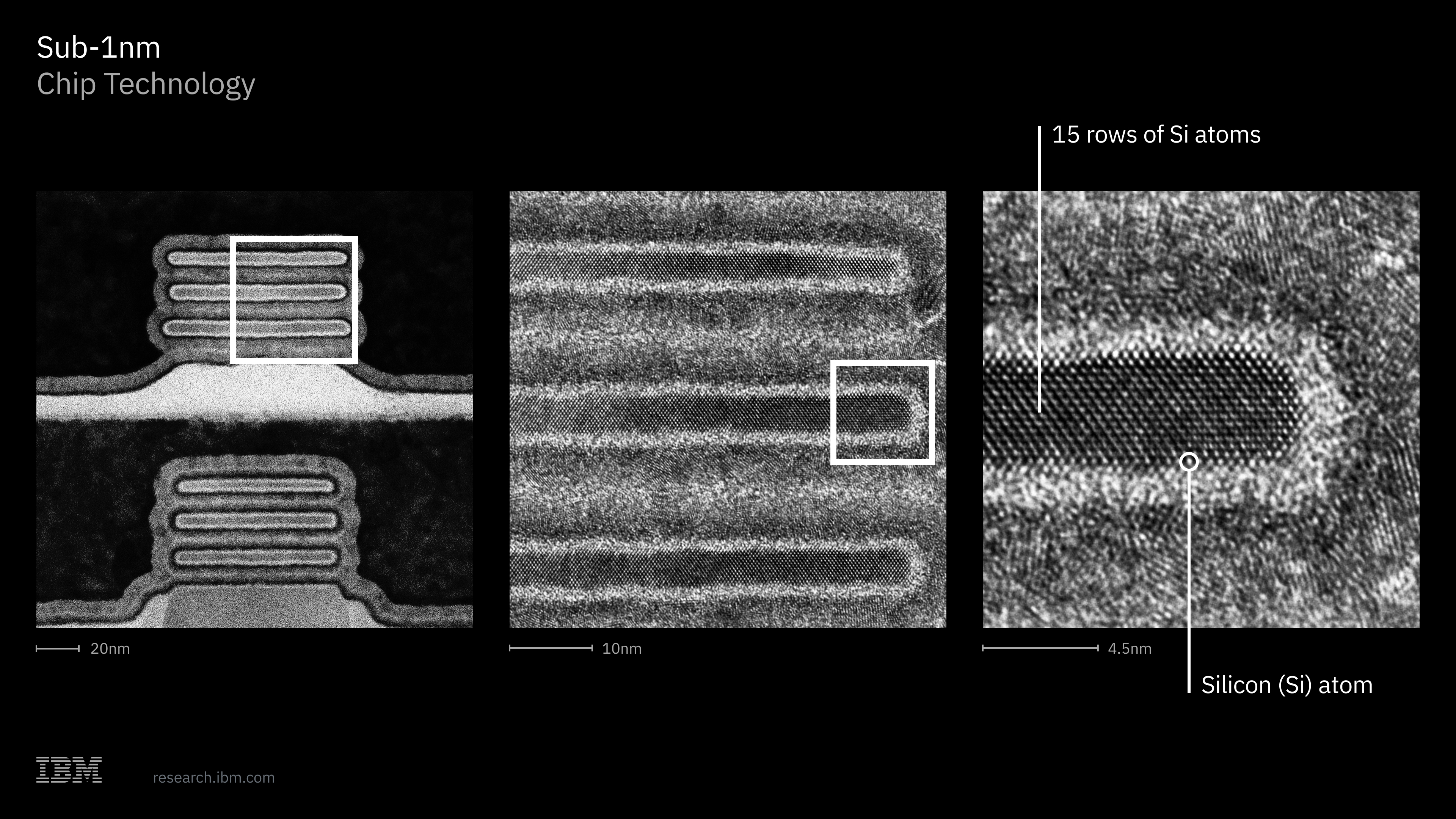
"Transistor nodes have shrunk dramatically, with leading developers like
IBM advancing into the sub-1 nanometre realm (e.g., 0.7-nanometer tech).
However, absolute limits are rapidly approaching due to several factors:
iirc terms like '5 nm process' no longer refer to any physical dimension
so I'm curious what the actual gate size is on 0.7 nm tech.
IBM sold their fab lines to GlobalFoundries and their '7 nm' tech was
closer to Intel's 10 nm.
On Tue, 30 Jun 2026 18:51:03 GMT, Charlie Gibbs wrote:
On 2026-06-30, c186282 <c186282@nnada.net> wrote:
On 6/30/26 09:51, Mr. Man-wai Chang wrote:
On 6/30/2026 5:14 PM, c186282 wrote:
Can you fabricate 0.000000...0000000001 nm chips?
Is zero the seal or wall?
ÿÿÿ Um, pretty quick you get to ATOMS ... and, for any normal
ÿÿÿ electronics, that's IT.
You cannot have 0.000000....00 nm chip.
That's a void, empty, nothing.
I tried to think through the implications of this but I got a divide
error.
"Shariputra, form does not differ from emptiness; emptiness does not
differ from form. Form itself is emptiness, emptiness itself form. Sensations, perceptions, formations, and consciousness are also like
this."
https://www.izauk.org/multimedia-archive/hannya-shingyo-the-heart-sutra/
Gate Gate Paragate Parasamgate Bodhi Svaha.
On Tue, 6/30/2026 12:06 PM, c186282 wrote:
On 6/30/26 09:51, Mr. Man-wai Chang wrote:
On 6/30/2026 5:14 PM, c186282 wrote:
Can you fabricate 0.000000...0000000001 nm chips?
Is zero the seal or wall? :)
ÿÿÿ Um, pretty quick you get to ATOMS ... and, for any
ÿÿÿ normal electronics, that's IT.
You cannot have 0.000000....00 nm chip.
That's a void, empty, nothing. :)
ÿ "Electronics" are now about literal atom-thick structures.
ÿ Can't go any smaller.
ÿ Any better future stuff will have to exploit quantum
ÿ effects - get more bang for yer nanometer. Alas quantum
ÿ stuff isn't as deterministic as bulk matter devices
ÿ and suffer from the uncertainty principle.
But only if there are properties that actually have some use.
A quick Google tells me there is a thing called "spintronics"
which can make insulators. The materials are "foreign" to
current semiconductors (so the materials may not "play nice"
with the rest of the substrate). And having an insulator,
does not give me a switching transistor.
Historically, we've made good use of quantum mechanical "tunneling",
which is finding a way underneath energy barriers. We have one
afternoon lab using one of these (these diodes are used in
time domain reflectometry for the nice sharp edges). I put mine right
across the terminals of an HP gray-plastic power supply, the one with
the course and fine controls. And you can use the power supply
as a curve tracer, and walk the diode right up to the
point where it switches. The power supply has amazing
characteristics at DC (not so much at HF). And that was
a fun afternoon of farting around.
https://en.wikipedia.org/wiki/Tunnel_diode
And that's an illustration of an effect, it's not me predicting
they'll run right out and make something out of that.
This is another example of tunneling.
https://en.wikipedia.org/wiki/Flash_memory#Fowler%E2%80%93Nordheim_tunneling
"The Fowler-Nordheim tunneling effect is reversible, so electrons
can be added to or removed from the floating gate, processes
traditionally known as writing and erasing."
There's no uncertainty principle there, you need enough electrons
to maintain noise immunity.
If there is some property that can be used, and is not a flaky pastry,
then it will be introduced slowly. There is too much money involved
for this to be just "science", it's "business" too. And that affects
how you do it.
On 6/30/26 19:28, rbowman wrote:
On Tue, 30 Jun 2026 16:27:24 +0100, The Natural Philosopher wrote:
"Transistor nodes have shrunk dramatically, with leading developers like >>> IBM advancing into the sub-1 nanometre realm (e.g., 0.7-nanometer tech). >>> However, absolute limits are rapidly approaching due to several factors:
iirc terms like '5 nm process' no longer refer to any physical dimension
so I'm curious what the actual gate size is on 0.7 nm tech.
IBM sold their fab lines to GlobalFoundries and their '7 nm' tech was
closer to Intel's 10 nm.
ÿ Well, SEEMS like they've done the 1, or <1, nm
ÿ stacked chip.
ÿ Umm ... so we're JUST MAKING IT UP.
ÿ Don't disagree for the most part. The Buddha,
ÿ even Plato to an extent, realized this 2500
ÿ years ago.
ÿ We YEARN for the anthropomorphic ... some hint
ÿ that the universe/reality cleaves to human-type
ÿ perceptions.
There's no uncertainty principle there, you need enough electrons
to maintain noise immunity.
ÿ Umm, no. "SpinTronics" may have uses - but, as you said,
ÿ it does not segway neatly with existing tech.
ÿ (fun - my spell-checker thing wants "Segway" - the
ÿ two-wheeled commercial thingie :-)
...
ÿ Existing transistor tech - it's deterministic, solid.
ÿ Alas with the IBM product we've probably reached the
ÿ bitter END of conventional electronics. Some seriously
ÿ different stuff will be needed for The Future if we
ÿ need more speed/density.
Apparently IBM has indeed BUILT these chips.
On Wed, 1 Jul 2026 10:05:05 +0100, The Natural Philosopher wrote:
Moses realized that giving them some relatively harmless shit would stop
a lot of argument.
His shit proved to be anything but harmless.
Historically, we've made good use of quantum mechanical "tunneling",
which is finding a way underneath energy barriers.
On Tue, 30 Jun 2026 22:09:52 -0400, Paul wrote:
Historically, we've made good use of quantum mechanical "tunneling",
which is finding a way underneath energy barriers.
Transistors wouldn?t work without that.
Heck, even vacuum tubes wouldn?t work without tunnelling.
vacuum tubes wouldn?t work without tunnelling.
On 2026-07-08 09:46, Lawrence D?Oliveiro wrote:
On Tue, 30 Jun 2026 22:09:52 -0400, Paul wrote:
Historically, we've made good use of quantum mechanical
"tunneling", which is finding a way underneath energy barriers.
Transistors wouldn?t work without that.
Heck, even vacuum tubes wouldn?t work without tunnelling.
Huh? Not sure I ever heard of that. Maybe my memory is failing.
On Wed, 8 Jul 2026 23:15:44 -0000 (UTC), Lawrence D?Oliveiro wrote:
But by regulating that energy barrier, you can modulate the amount of
particle current that crosses it, over a continuous range from off to
low to high, as opposed to completely off versus completely on. This
only works because of quantum theory.
It's amazing how many things worked quite well prior to someone developing
a theory.
| Sysop: | Jacob Catayoc |
|---|---|
| Location: | Pasay City, Metro Manila, Philippines |
| Users: | 4 |
| Nodes: | 4 (0 / 4) |
| Uptime: | 496009:05:20 |
| Calls: | 178 |
| Files: | 605 |
| D/L today: |
22 files (18,741K bytes) |
| Messages: | 70,143 |